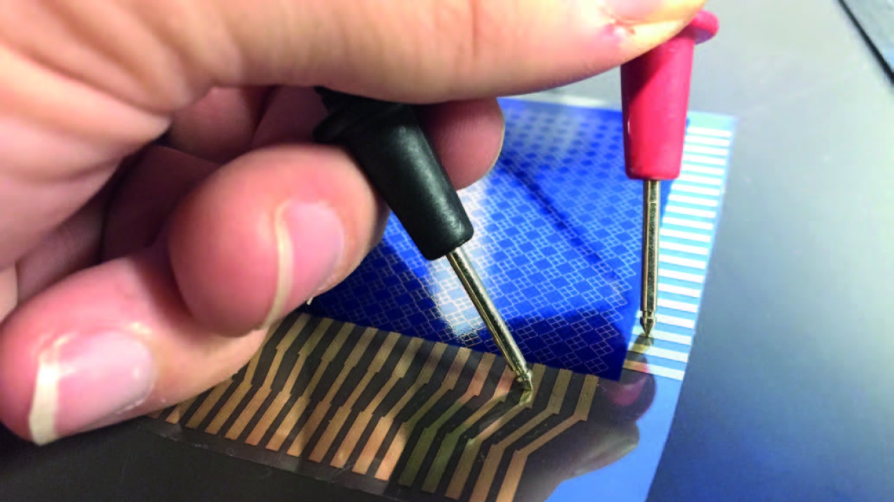
FTA presents flexible printed touch interface

Flexo printed touch interface
Clemson University student Nathan Pretorius told delegates how he had used Rossini scholarship funds to successfully print a flexographic capacitive touch interface.
Pretorius submitted his concept for a printed electronics project to the Rossini North America Flexographic Scholarship Competition in 2014 and was awarded first place. With the money, Pretorius worked on building a mutual capacitive touch interface using flexographic printing rather than screen printing.
The printed touch pad was designed with a matrix of capacitive sensing nodes arranged in an XY coordinate system to detect when a finger is touching a surface (similar technology to what’s used in smart phones today). The flexo design has four times as many sensors, can sense multiple touch points and uses less ink than a screen printed piece.
The most critical design consideration was the relationship between line thickness and conductivity and the smallest line that could be reliably printed. Pretorius selected a diamond shape because it optimizes the surface area when there are two layers of sensing lines that need to be equally visible. In the print layout, two layers of perpendicular lines are separated by a dielectric, or non-conductive material. When a finger touches the surface, it changes the discharge time of the resistor-capacitor time circuit because of the body’s capacitance, or ability to store an electric charge. He said, ‘For electrical considerations, all lines must be continuous. The dielectric ink film thickness is ideally as thin as possible without allowing shorts, but silver thickness doesn’t matter as much. One break in the dielectric can ruin an entire sensing line.’
In the process, first a silver ink layer is printed, then a UV ink is printed and cured followed by a second layer of silver ink. The layers run through a tunnel dryer at 350 degrees F and then a final layer of UV varnish is applied as an extra insulating layer.
The solid dielectric made of generic UV ink serves as a bridge. The highly conductive silver used was PChem PFI-722 nanoparticle water-based flexo ink. Adjustments needed to be made in the design because it proved difficult to cure the silver ink using a normal water-based drying system. The dryers must be able to sinter, or bond, the conductive ink layers in a single pass.
The final design trial used a 500 LPI at 5.5 BCM anilox for the dielectric layer, which completely insulated the conductive layers. Pretorius produced a functioning capacitive touch interface in one pass at 75ft/min using an in-line tunnel dryer on an Omet Varyflex.
Pretorius explained that one of the major production issues was the print moving out of register as it came out of the on-press tunnel dryer. Registration is crucial for correct capacitance. He found it difficult to keep the registration between the vertical sensors, solid dielectric and horizontal sensors in stations one, two and three. For commercial applications, it would be necessary to regularly check for shorting between layers during production.
Nathan Pretorius will pursue his interest in Printed Electronics in graduate school this fall. Watch a video here: https://goo.gl/fsPlQe
Stay up to date
Subscribe to the free Label News newsletter and receive the latest content every week. We'll never share your email address.

